Applications
Latest Applications
Complex and delicate structure
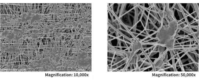
Lignocellulosic nanofibers
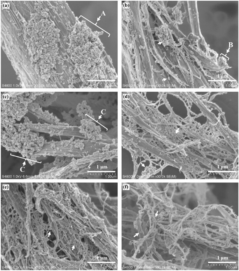
The lignocellulosic nanofibers, characterized by their ultrafine and intricately structured morphology, are uniformly coated with osmium, enabling the acquisition of clear, high-resolution SEM images without charging. Additionally, the automatic thickness adjustment function ensures reproducible coating.
Data provided by the National Institute of Advanced Industrial Science and Technology (AIST), Chugoku Center, Materials and Chemistry Area, Functional Chemistry Research Department, Cellulose material group, Takashi Endo, Keita Sakakibara, Yasuko Saito
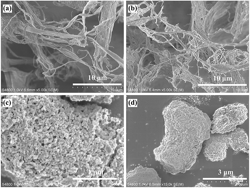
(Left images) a. Lignocellulosic microfibers, b. Lignocellulosic nanofibers, c&d. Quinacridone
(Right images) Mixture of quinacridone and lignocellulose MF: a 2:1 (w/w), b 1:9 (w/w). Mixture of quinacridone and lignocellulose NF: c 2:1 (w/w), d 1:1 (w/w), e 1:4 (w/w), f1:9 (w/w). Arrows indicate quinacridone particles.
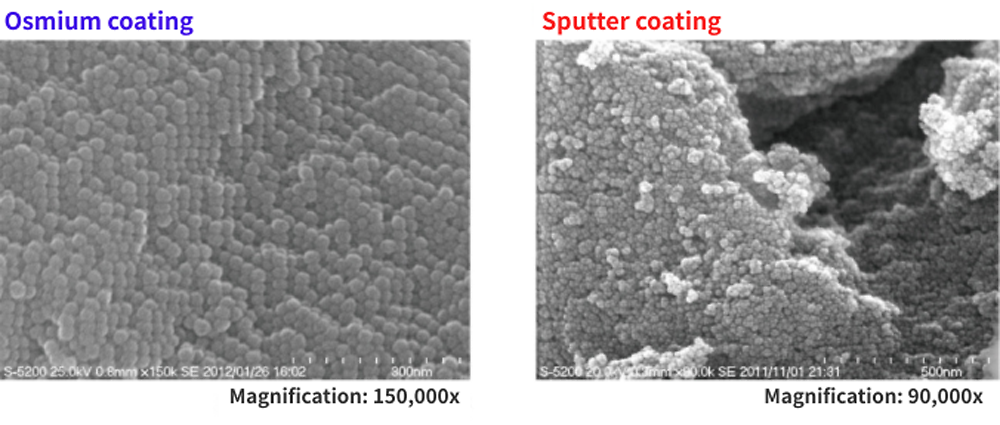
Osmium vs. Sputter Coating
Discrimination of nanoparticles in high-magnification observation
Silica nanoparticles
Osmium coating enables clear discrimination of silica nanoparticles at up to 150,000x by eliminating charging effects and providing superior coating compared to conventional gold sputtering, which often obscures the underlying silica particles due to the presence of gold coating.
Data provided by Nagoya University, Graduate School of Engineering, Advanced Physical Chemistry, Daisuke Kawaguchi
Optimal SEM observation with an ultrathin, non-granular film
HB tubes (SiO2 Al2O3)
Data provided by Nagoya University, Technical Center, Shoji Takai
Clear imaging of intricate tip structures
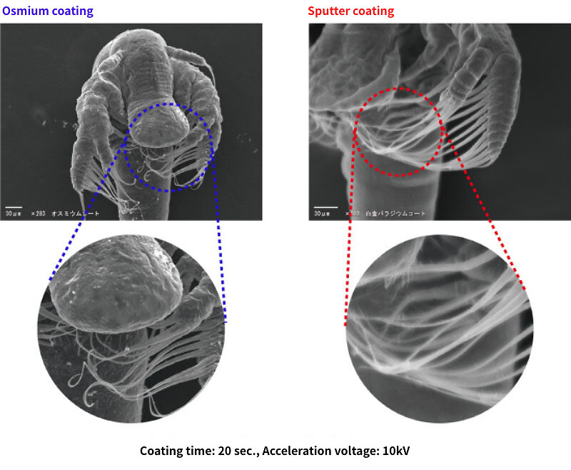
Artemia larvae (Sea Monkey)
Freeze-dried Artemia larvae (Sea Monkey) are coated with sputter and osmium coating for SEM observation. Osmium coating provides a striking three-dimensional image, allowing for clear observation of the intricate tip structures of the antennae, which are obscured by charging artifacts in the sputter-coated sample.
Data provided by Kitasato University, School of Allied Health Sciences, Masaki Ueno
Unveiling the original structure obscured by gold sputtering
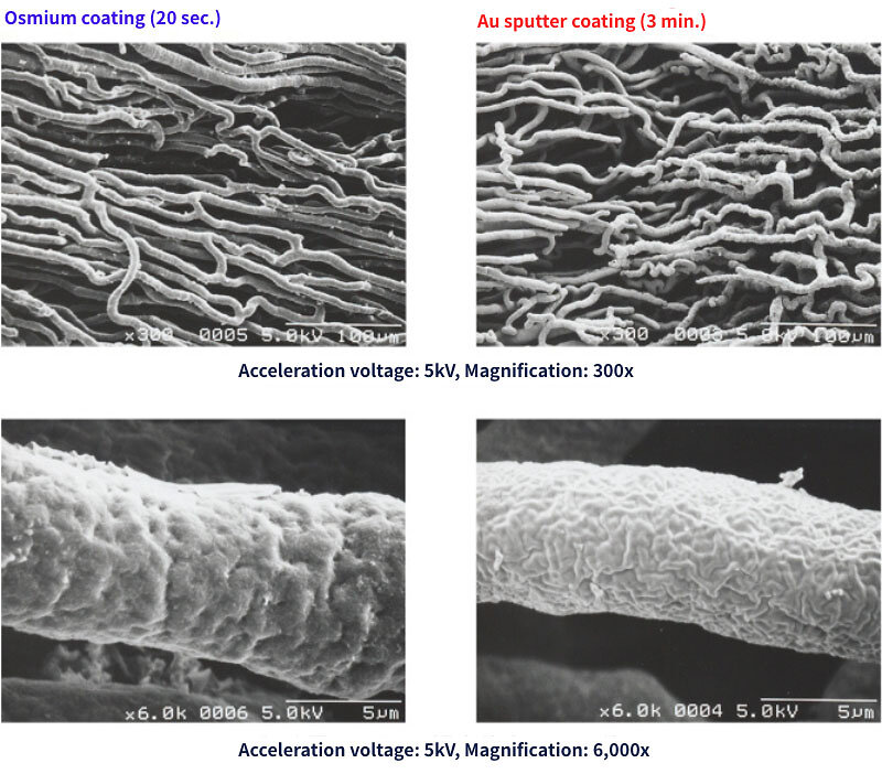
Comparative imaging of rat heart vascular casts
Gold sputtering requires approximately 3 minutes of coating to minimize charging, and this prolonged process often results in heat damage, causing shrinkage and a thick, uneven coating that can obscure fine surface details. In contrast, osmium coating produces a thin, uniform film in just 20 seconds, eliminating charging artifacts and enabling high-resolution imaging of the sample’s true morphology. At 6,000x, the difference in surface morphology between the two coating methods is evident.
Data provided by Okayama University, Graduate School of Medicine, Dentistry and Pharmaceutical Sciences, Department of Human Morphology
Osmium coating prevents charging artifacts, allowing for clear imaging of overlapping samples
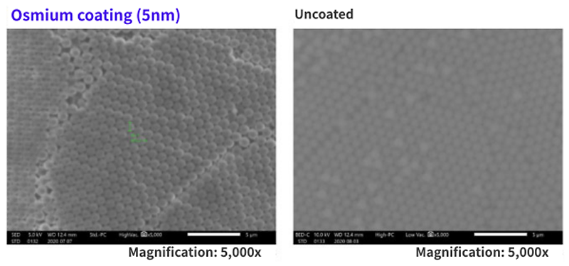
Polystyrene particles #1
A 5nm osmium coating provides superior image quality for overlapping 800nm polystyrene particles compared to uncoated samples. The osmium coating effectively eliminates charging artifacts, allowing for clear observation of individual nanoparticles.
Data provided by Toyohashi University of Technology, Electronic Materials Course, Hiroyuki Muto
Polystyrene particles #2
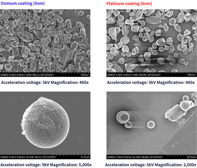
Our osmium coating systems provide excellent coating coverage, even on overlapping samples, effectively preventing charging and enabling high-contrast observation of the entire sample. On the other hand, gold sputtering often results in charging, particularly in overlapping areas due to poor coating.
This limits the maximum magnification to around 2000x. However, osmium coating allows for high-resolution imaging even at 5000x, revealing fine details.
Data provided by Toyohashi University of Technology, Electronic Materials Course, Hiroyuki Muto
Achieving enhanced stability and high-resolution imaging
Carbon nanotubes
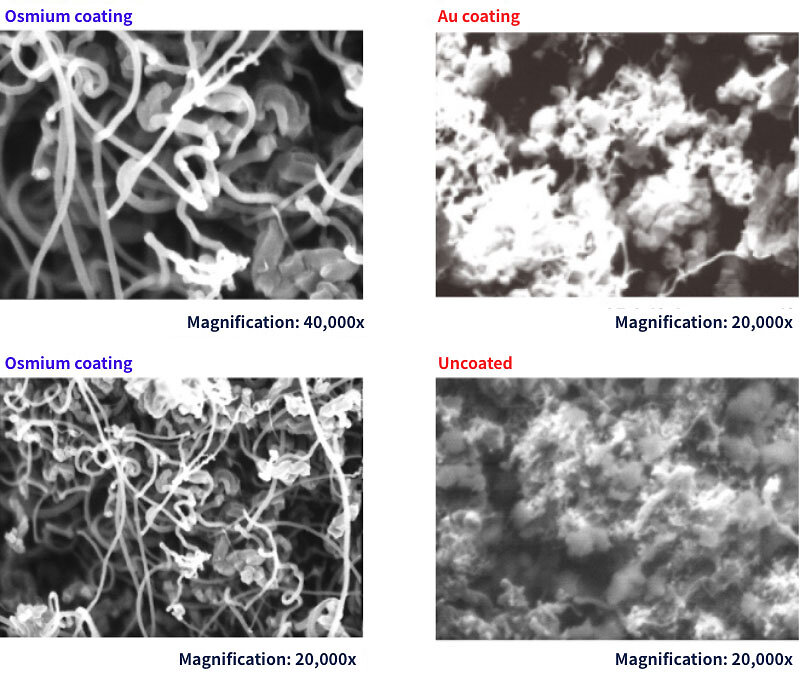
Even carbon nanotubes observable by SEM without deposition can benefit from osmium coating, which enhances their stability and enables high-resolution observation. The observation of uncoated carbon nanotubes can result in their diffusion and subsequent contamination of the SEM detector. However, osmium coating is resistant to electron beam, and prevents diffusion.
It not only acts as an antistatic film but also prevents SEM detector contamination by inhibiting carbon nanotube diffusion.
Data provided by Meijo University, Faculty of Science and Technology Department of Materials Science and Engineering, Tomoko Suzuki (Former member of Ando Laboratory)
Observing without damaging the matrix structure
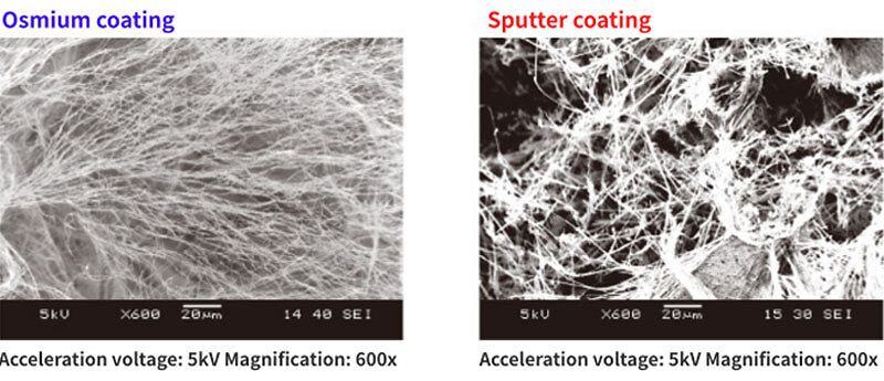
The solid-state structure of freeze-dried amino acid cakes is observed at 600x without any damage to the matrix.
Conventional platinum sputtering often results in unclear observation of the porous structure of freeze-dried cakes, with limited depth of field and damage to the matrix due to the weight of the sputter particles. In contrast, osmium coating, with its thin and conformal nature, enables clear observation of the intricate matrix structure of freeze-dried cakes without causing damage.
Data provided by Tokyo University of Science, Faculty of Pharmaceutical Sciences, Formulation Science, Yamashita Chikamasa
No granularity even at high magnification
Polymer films
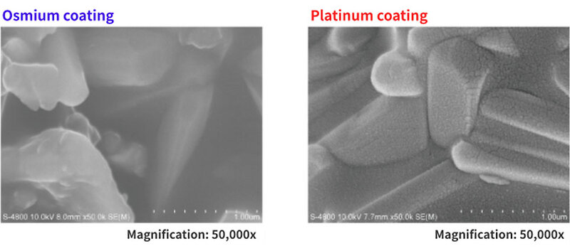
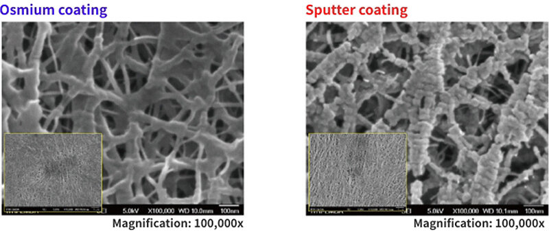
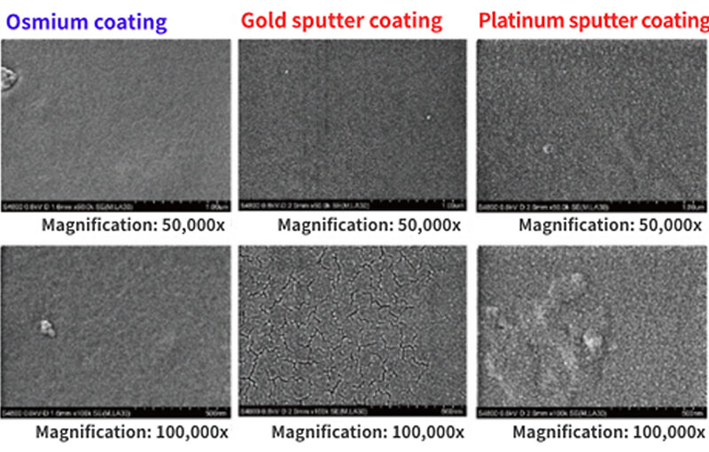
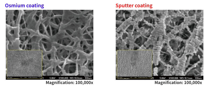
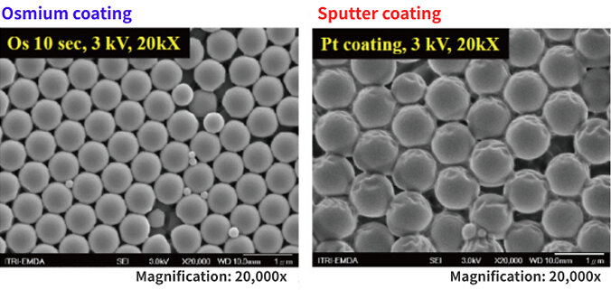
At 100,000x, osmium coating provides a smooth surface without any granular artifacts, allowing for clear observation of the true surface structure. In contrast, platinum coating results in a granular surface, obscuring the underlying structure.
Osmium coating enables high-resolution imaging without the granular artifacts commonly associated with platinum coating. Additionally, the low applied voltage prevents heat damage to organic samples.
Data provided by Industrial Technology Research Institute (Taiwan)
Clear difference even at low magnification
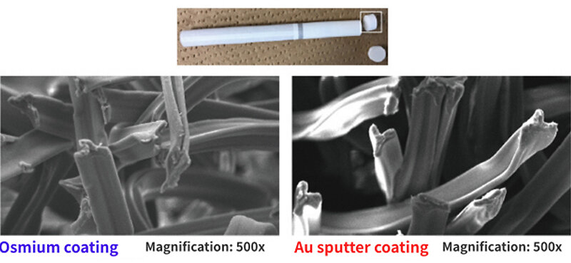
Acetate
Even at low magnification, the difference in surface quality between gold-sputtered and osmium-coated acetate samples is evident. Gold sputtering results in a metallic appearance and charging artifacts, while osmium coating preserves the original surface texture and allows for clear observation.
Comparison of three coating methods: osmium coating, gold sputtering, and platinum sputtering
SiC wheels
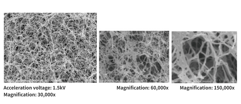
Achieving nanometer-scale resolution
Observing deep into nanofibers
Cellulose nanofibers
Conventional sputtering methods often result in poor coating coverage, making it difficult to obtain clear images of nanofibers. In contrast, osmium coating provides excellent coating, allowing for the observation of even the finest nanofibers without breakage.
Data provided by the National Institute of Advanced Industrial Science and Technology (AIST), Bioproduction Research Institute, Seung-Hwan Lee
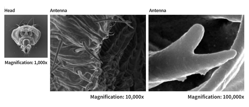
Drosophila
Osmium coating enables high-resolution imaging of samples without inducing any structural damage, even at 100,000x. This technique is particularly beneficial for heat-sensitive and fine-structured samples, as it eliminates the granular appearance and electron beam damage commonly associated with other coating methods.
Data provided by Tohoku University, Institute of Multidisciplinary Research for Advanced Materials (IMRAM), Yoshiro Shibata
Coal ash
Clear, high-resolution images of rough-surfaced samples, such as coal ash in cement, can be obtained with osmium coating, eliminating charging artifacts even at 150,000x.
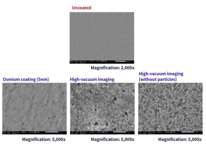
0.22 μm millipore filters
Osmium coating enables high-quality, three-dimensional imaging of samples, even under low-vacuum conditions, without charging artifacts. While uncoated samples are difficult to observe beyond 2000x due to charging under low vacuum conditions, osmium coating enables clear observation of filter structures even at 5000x.
Even challenging samples including filters that are difficult to image under low vacuum conditions can be clearly visualized by switching to high vacuum mode after osmium coating.
The image below shows that the structure is complex and intricate, designed to capture fine particles.
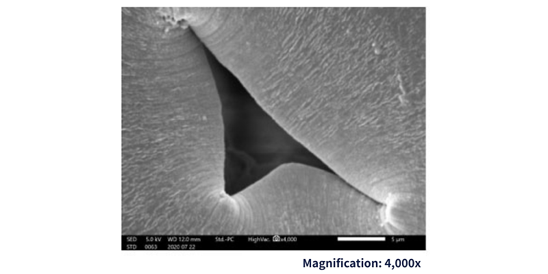
Polyurethane nanopores
The three-dimensional structure of the surface, including pores as small as a few micrometers in diameter, can be clearly observed.
Fully coating even complex samples
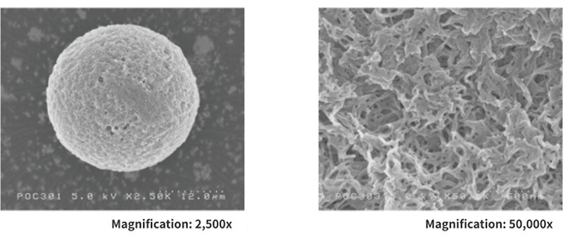
Sepharose
Sepharose, a type of polymer bead commonly used for adsorption of biological samples such as proteins and microorganisms, has a porous surface.
Osmium coating can coat the deep pores, enabling clear observation of complex structures even at high magnification without granular artifacts.
Fossils
Even porous samples can be observed clearly.
Data provided by Tohoku University, Institute of Multidisciplinary Research for Advanced Materials (IMRAM), Yoshiro Shibata
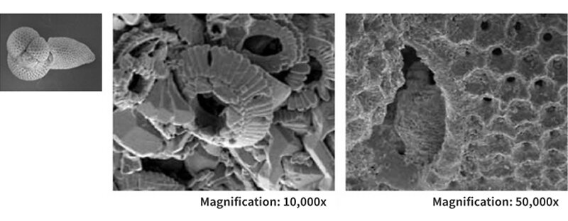
Star sand
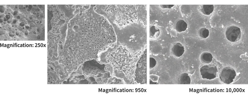
Star sand, primarily composed of calcium carbonate, has a porous surface. Sputter coating fills the surface irregularities, making it difficult to observe the fine structures at high magnification. The 10,000x image provides a more in-depth view of the pore structure than the 950x image.
Data provided by JEOL Ltd.
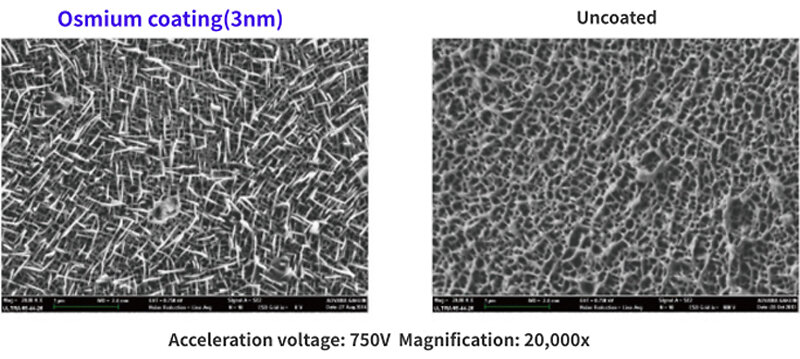
Green lacewing wings
The images compare uncoated and osmium-coated green lacewing wings observed under low-acceleration SEM. The uncoated sample exhibits significant electron beam damage, obscuring the delicate, needle-like structures. In contrast, the osmium-coated sample shows minimal damage, allowing for clear observation of the original, fine structures.
The osmium coating is also resistant to heat damage, making it suitable for heat-sensitive materials such as resins and biological samples.
Data provided by Aoyama Gakuin University, College of Science and Engineering, Akito Takashima, Reona Takahashi
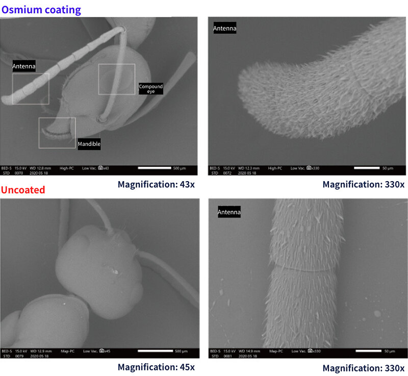
Ants
Osmium coating allows for detailed observation of the ant’s body surface, revealing fine structures such as the outline and texture of the antennae.
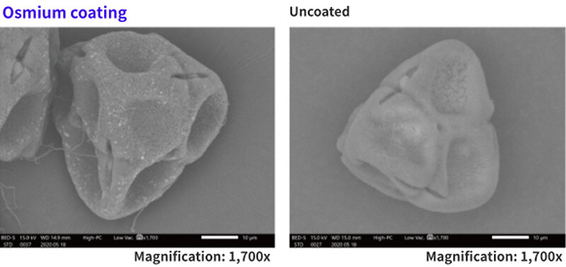
Azalea pollen
Compared to the uncoated sample, the osmium-coated sample provides a clearer image with sharper edges and more distinct surface features.
Osmium coating is also effective for low-vacuum SEM, and it does not cause heat damage, allowing for clear observation of delicate structures such as the adhesive threads of azalea pollen without damage.
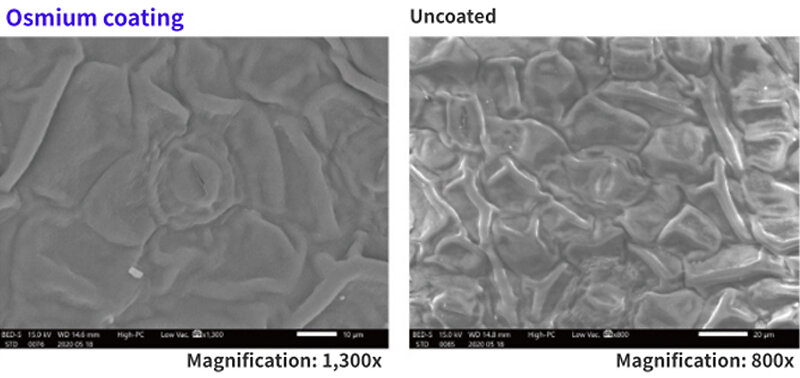
Stomata of azalea leaves
The uncoated azalea leaf exhibits charging artifacts at 800x, while the osmium-coated sample allows for clear observation of stomata at 1300x.
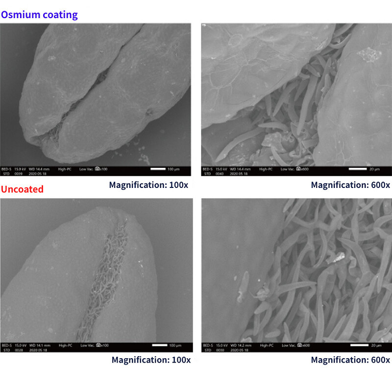
Rosemary leaves
Osmium coating enables the imaging of detailed structures such as surface morphology and the depth of the internal trichomes.
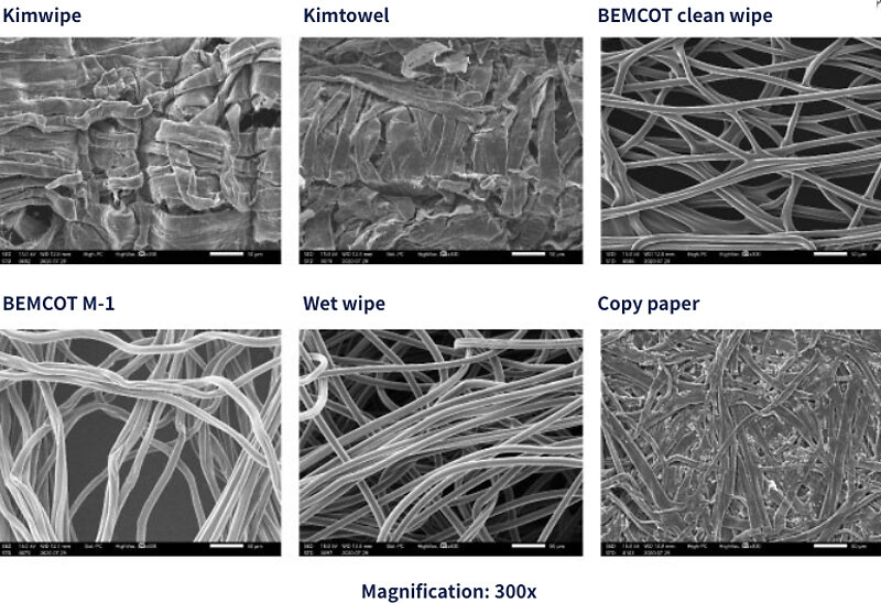
Common textile materials
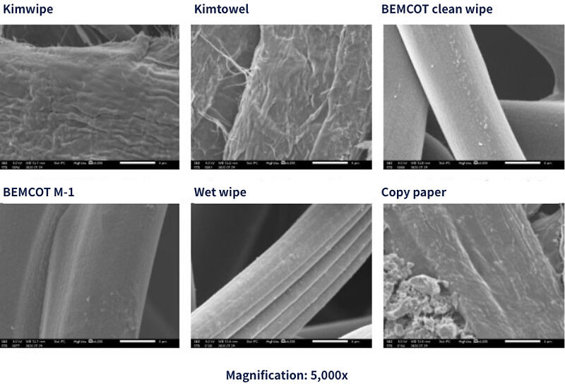
A comparative study of various fibrous materials is conducted using low-magnification SEM.
Significant differences in the microstructure are observed in pulp-based products (Kimwipes, Kimtowels, copy paper) and synthetic fiber products (BEMCOT clean wipes, M-1, wet wipes).
Variations in weave structure are observed between Kimwipes and Kimtowels, and differences in fiber entanglement are shown between BEMCOT clean wipes and M-1, despite being made from the same material. Wet wipes contain fibers with grooves for water absorption, and copy paper shows the presence of calcium and silicon fillers as loading materials. Observation at 5,000x can be easily achieved using only the auto-focus function of a benchtop SEM.
Even heat-sensitive samples remain undamaged
Membrane filters
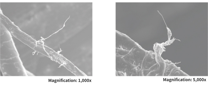
Delicate membrane filters, prone to heat damage, can be effectively imaged using osmium coating without compromising their structural integrity.
Wolf’s fur
The wolf’s fur exhibits no signs of heat damage. The barbed, frayed hairs, susceptible to heat, would typically curl or distort with sputtering.
Titanium implant surfaces
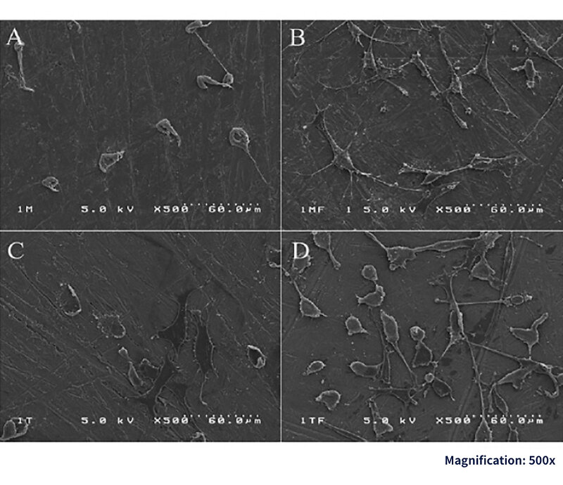
Most dental implant bodies are made of titanium. The titanium surface of these implant bodies undergoes various treatments such as sandblasting, acid etching, and hydroxyapatite coating in addition to mechanical polishing. These surface treatments increase the contact area between the implant body and the surrounding bone, and at the cellular level, changes in the microstructure and chemical composition of the titanium surface promote adhesion and proliferation of osteoblasts. In this field of research at the Nippon Dental University, osmium coating has been used as a preparation method for SEM observation after surface treatment of titanium.
The following is an SEM image of a titanium surface functionalized with H2O2 hydrothermal oxidation and FGF-2, 24 hours after cell seeding. Cellular adhesion is evident, with no detachment of filopodia.
Data provided by The Nippon Dental University, School of Life Dentistry, Tomonori Matsuno
Polymer beads
Under the same observation conditions, beads coated with platinum show significant electron beam damage on the surface. On the other hand, osmium coating provides clear imaging with no damage or charging, even though it is a thin film.
Data provided by Industrial Technology Research Institute (Taiwan)
Applications in various analyses
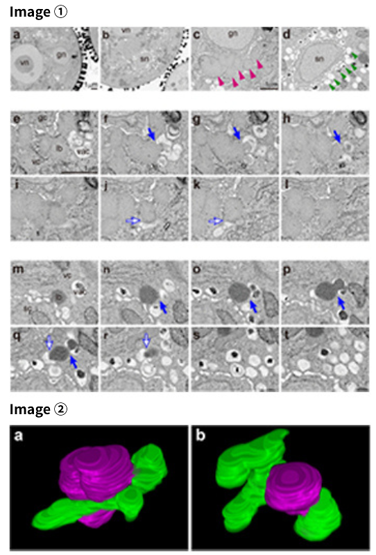
Ultrathin pure osmium coating in serial section SEM (Analysis of microlipophagy during pollen maturation in Arabidopsis thaliana)
Serial section SEM method, also known as array tomography, is a technique that enables easy 3D reconstruction by observing continuous ultrathin sections using a scanning electron microscope. In this publication, after fixation and resin embedding, the samples are sectioned using an ultramicrotome, coated with osmium, and observed with a field emission scanning electron microscope. Subsequent 3D reconstruction through image processing enables to analyze fine organelle interactions and reveal the involvement of microlipophagy in pollen maturation in Arabidopsis thaliana.
The osmium coater enables the reproducible formation of highly conductive, ultrathin pure osmium films less than 1 nm thick, ideal for backscattered electron imaging to visualize tissue changes and surface topography. Its non-granular nature allows for the observation of the intrinsic material structure, making it a perfect choice for preparation for serial section SEM.
Image ① Ultrastructural analysis of interactions of vacuoles and lipid bodies by serial section SEM
a–d SEM images of bicellular pollen (a, c) and tricellular pollen (b, d)
e–t Serial section SEM images of the bicellular stage (e–l) and the tricellular stage (m–t)
gc: generative cells, gn: generative nuclei, lb: lipid bodies, sc: sperm cells, sn: sperm nuclei, vac: vacuoles, vc: vegetative cells, vn: vegetative nuclei
Image ② 3D reconstructed images of microlipophagy
a and b are 3D images in the bicellular stage created from Image ① e-l and the tricellular stage created from Image ① m-t, respectively. Magenta structures indicate lipid bodies, and green structures indicate vacuoles
Data provided by Japan Women’s University, Faculty of Science, Department of Chemical and Biological Sciences, Noriko Nagata, Kae Akita
Images: Figures 4 and 5 in the following link
https://link.springer.com/article/10.1007/s00709-020-01557-2
Original article: Kae Akita, Tomoko Takagi, Keiko Kobayashi, Kazuyuki Kuchitsu, Tsuneyoshi Kuroiwa & Noriko Nagata (2020) Ultrastructural characterization of microlipophagy induced by the interaction of vacuoles and lipid bodies around generative and sperm cells in Arabidopsis pollen.
A 0.25 nm conductive coating is highly effective for precise EBSD surface analysis
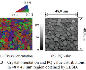
Lead zirconate titanate polycrystal
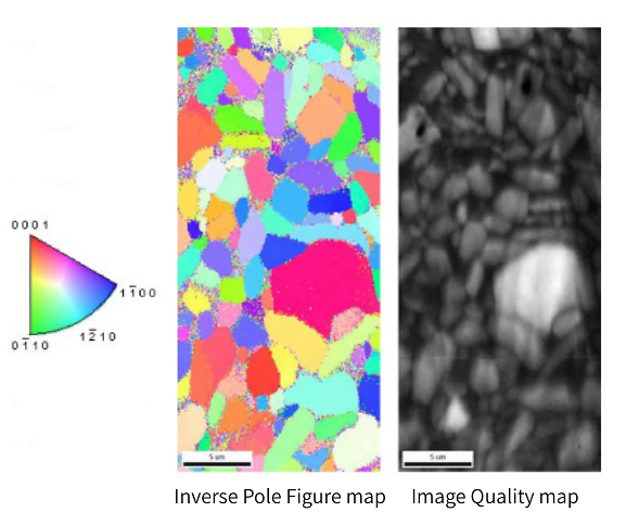
Pure osmium’s excellent conductivity and secondary electron emission efficiency prevent charging. This has enabled high-resolution analysis over a wide area of insulating samples, which was previously difficult due to charging caused by electron beam irradiation. The results demonstrate that even an ultrathin osmium coating of 0.25 nm is sufficient to completely shield the sample from the electron beam and provide high-quality backscattered electron data, allowing for detailed analysis of crystal structures such as grain boundaries.
Reference: Transactions of the Japan Society of Mechanical Engineers. Volume 74, No. 739, A
Osaka Institute of Technology, Department of Mechanical Engineering, Yasutomo Uetsuji
Improving the durability of AFM cantilevers
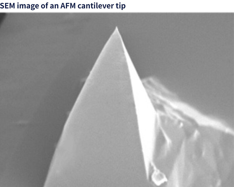
Theoretically, the tips of SPM/AFM cantilevers are exposed to extremely high electric fields. Consequently, gold-coated cantilevers frequently experience substantial damage after only a few measurements, rendering them unusable. In contrast, cantilevers coated with osmium exhibit significantly enhanced durability. This allows for the effective reuse of these costly cantilevers.
Data provided by the National Institute of Advanced Industrial Science and Technology (AIST), Tohru Nakamura
Realizing quantitative analysis through EDS
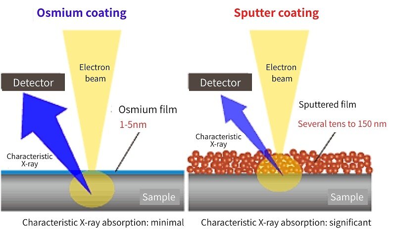
Gold sputtering has been the standard for anti-charging in EDS analysis of low atomic number elements like carbon. However, gold films absorb characteristic X-rays, hindering accurate quantitative analysis. Our plasma CVD technology enables the deposition of uniform, ultrathin osmium films, which have minimal X-ray absorption and do not interfere with quantitative analysis. This makes it particularly suitable for the analysis of light elements such as carbon and nitrogen.
Reference: “EDS quantification of light elements using osmium surface coating”
Journal of Mineralogical and Petrological Sciences, Volume 110, page 189-195,2015
Ultrathin films exhibiting significantly enhanced mechanical strength compared to carbon FIB films
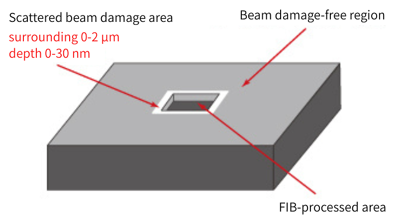
Scattered ions during FIB milling can cause damage to the surrounding area. Osmium coating is an effective preparation to protect the damaged area. By eliminating the damage, high-resolution analysis of the outermost surface can be performed at the nanoscale.
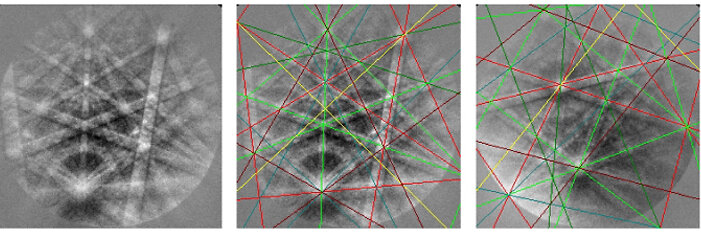
Osmium coating for anti-charging in EBSD
Alumina plate (approximately 50×70×4mm t)
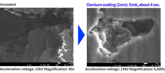
SEM observation results: The uncoated sample exhibits severe charging, preventing observation. However, osmium coating provides excellent coverage, eliminating charging even in deep cavities.
EBSD observation results: Measurements are taken with the sample tilted at approximately 70 degrees.
User feedback
“For EBSD analysis of non-conductive materials, a conductive coating is needed that does not hinder the detection of backscattered electrons from near-surface crystals and is stable under electron beam irradiation. Osmium coating provides a thin, conductive layer that enables the acquisition of high-quality Kikuchi lines. Its excellent coating uniformity prevents charging, even in samples with pores.”
Sample preparation for FE-EPMA analysis
In-vehicle dust
User feedback
“Exposure to contaminants through in-vehicle dust has raised concerns. Given that dust contains a mixture of organic and inorganic contaminants, conventional analysis methods require complex preparation and multiple instruments. To address this, the Masunaga Laboratory at Yokohama National University developed a simplified method using a Field Emission Electron Probe Micro Analyzer (FE-EPMA) to analyze the elemental composition of in-vehicle dust (Environmental Science 30[1] 34-43, 2017). Osmium coating was employed as a sample preparation step. EPMA is an analytical tool that utilizes the detection of characteristic X-rays emitted from a sample surface upon electron beam irradiation to perform elemental analysis and quantification. It can simultaneously analyze both organic and inorganic contaminants, making it well-suited for analyzing small samples like dust.”
Coating conditions:
Dust samples are mounted on a sample stage using carbon tape
Vacuum: 0.5 to 1 Pa
Current: approximately 10 mA
Coating time: 20 to 25 seconds
Film thickness: approximately 10 to 12.5 nm
Data provided by Yokohama National University, Graduate School, Faculty of Environment and Information, Sciences, Shigeki Masunaga
FE-EPMA analysis of in-vehicle dust, including secondary electron imaging (SEI), backscattered electron imaging (BEI), and elemental color mapping
Osmium coating enables the analysis of multiple elements and is effective as a sample preparation method for FE-EPMA.
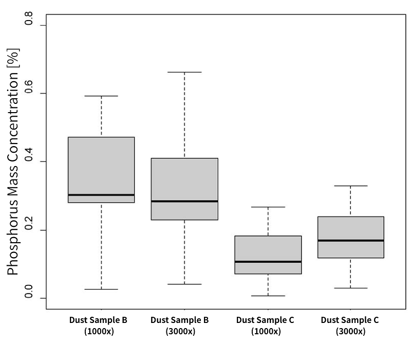
Quantitative analysis results of phosphorus by FE-EPMA
Quantitative analysis of phosphorus is successfully performed.
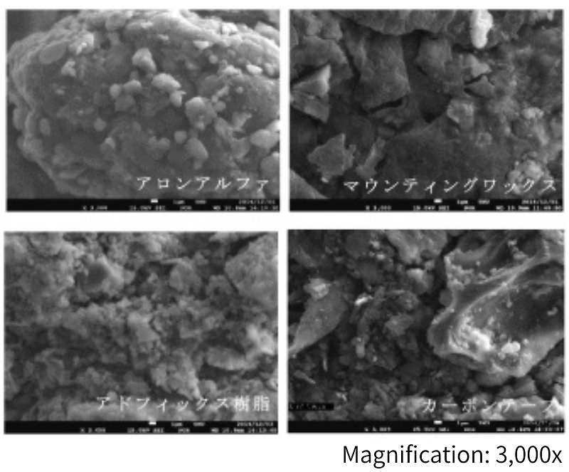
Comparison of secondary electron images obtained by FE-EPMA for in-vehicle dust samples prepared using different fixation methods
Good observation results are obtained even for samples with uneven surfaces.
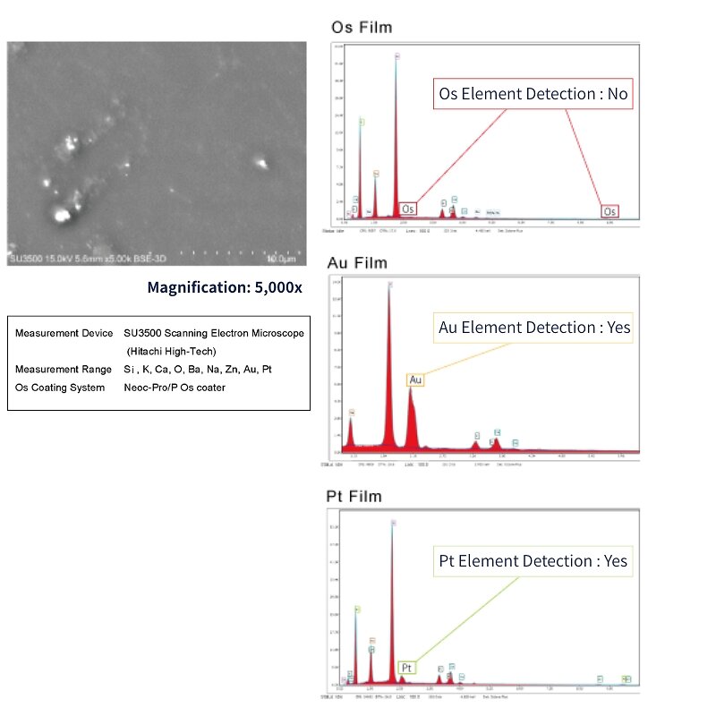
Energy Dispersive X-ray Spectroscopy
Energy dispersive X-ray spectroscopy (EDS) analysis is performed on a glass slide coated with an osmium film less than 1 nm thick. While gold and platinum elements are detected, respectively, osmium is not detected in the EDS spectrum, indicating that it does not interfere with the analysis.
FIB processing
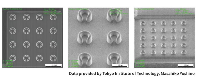
Molds for metamaterial fabrication examples/ SIM images
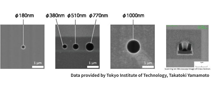
An osmium metal film is used as a protective coating prior to FIB processing. The high conductivity and thermal dissipation of the osmium film effectively shields the sample surface from FIB damage. Moreover, the osmium film can be easily removed using hypochlorous acid, allowing for further analysis of the sample after FIB processing.
SIM images of nanopores drilled in a 4 μm thick glass substrate using FIB