 |
 |
 |
Imaging
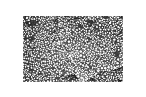
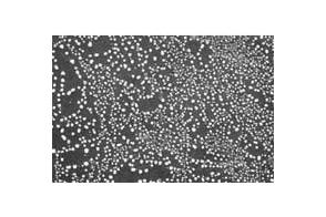
Unlike in TEM, there are no objective and projection lenses in SEM. We refer to this as a multi-stage condenser lens system, whereby the end lens is responsible for the intensive bundling of the primary electron beam. The diameter of this point-shaped beam, along with the material composition of the sample, determines the resolution capacity. In the ideal case, the resolution limit is 1- 2nm. A high resolution can only be expected with a circular beam. If astigmatism occurs due to lens aberrations, resolution standards (gold islands, tin islands) should be used for correction. This also applies for image distortion effects caused by the generally tilted specimen in the beam path. The correction of image aberrations is an important requirement for morphometric analyses. Generally, the SEM works with an electrical voltage of up to 30kV. The scanning of the sample point by point and line by line results in the scattering of primary electrons and release of secondary electrons, which are measured in electron detectors. The measured current per pixel is converted electronically into high-resolution images then. Element analyses can also be carried out in the SEM due to the emitted X-rays. In this case, an EDX detector (energy dispersive X-ray spectroscopy; EDX) is used. Special EDX calibration standards are used to check the position of the EDX spectra and the detector performance.