 |
 |
 |
Coating
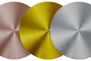
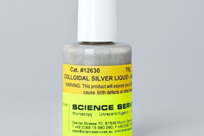
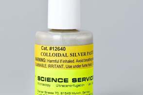
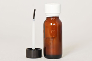
Biological samples and many other materials such as plastics, textiles and glass are electrical non-conductors (insulators). For imaging in SEM, a surface should ideally be conductive to avoid local charges and to produce a high number of detectable secondary electrons. The solution to this problem are thin electrically conductive layers, such as gold, platinum, palladium or carbon (graphite), which are sputtered with the help of a sputter coater and deposited on the dry samples. It is also important that all samples have good electrical contact with the sample plates. Various conductive adhesives can be used for this, such as conductive silver and carbon glue or carbon tape.