FOCUS ON... COATING METHODS
To make samples conductive for electron microscopy (EM), several coating methods are employed. These techniques are essential for preventing charging artifacts during imaging with electron beams and for improving image resolution and contrast. The choice of coating method depends on the nature of the sample and the intended application. Below is an overview of common coating techniques used in EM sample preparation:
1. Sputter Coating involves the bombardment of a target material, such as gold, gold-palladium, or platinum, with argon ions.
This ion bombardment ejects atoms from the target, which then condense onto the sample surface to form a thin, conductive layer.
This method is widely used for coating non-conductive SEM samples to enhance conductivity and prevent charging.
- Advantages: Provides uniform and quick coatings, is easy to operate, and suitable for routine SEM use.
- Disadvantages: The resulting coating may have a coarse grain size, which could obscure fine surface details at high magnification.
2. Carbon Coating uses vaporized carbon, typically deposited through resistance heating or electron beam evaporation in a vacuum, to form a conductive film on the sample. This method is favored for high-resolution imaging where a minimal interference coating is required.
- Advantages: Produces thin, uniform, and chemically inert layers ideal for high-resolution SEM.
- Disadvantages: Less conductive than metals and requires specialized, often more complex, equipment.
3. Thermal Evaporation involves heating a coating material in a vacuum until it evaporates. The vapor condenses onto the sample surface to form a thin film.
- Advantages: A simple and fast method for coating with a range of materials.
- Disadvantages: Coatings may be uneven, reducing precision compared to other methods like sputtering.
4. Electron Beam Evaporation - in this method, a high-energy electron beam is used to heat and evaporate a coating material.
The evaporated atoms then condense on the sample surface.
- Application: Suitable for high-purity and precision coatings, including tungsten.
- Advantages: Offers precise control over thickness and produces coatings of high purity.
- Disadvantages: More expensive and complex, requiring advanced equipment and careful control.
5. Plasma Enhanced Chemical Vapor Deposition (PE-CVD) involves the use of plasma to activate gaseous precursors, which then chemically react on the sample surface to form a solid coating. It is particularly effective for samples with complex topographies or delicate structures.
- Advantages: Allows very thin and uniform layers to be deposited with minimal energy transfer, making it suitable for fragile samples.
- Disadvantages: Requires specialized equipment and reactive chemicals.
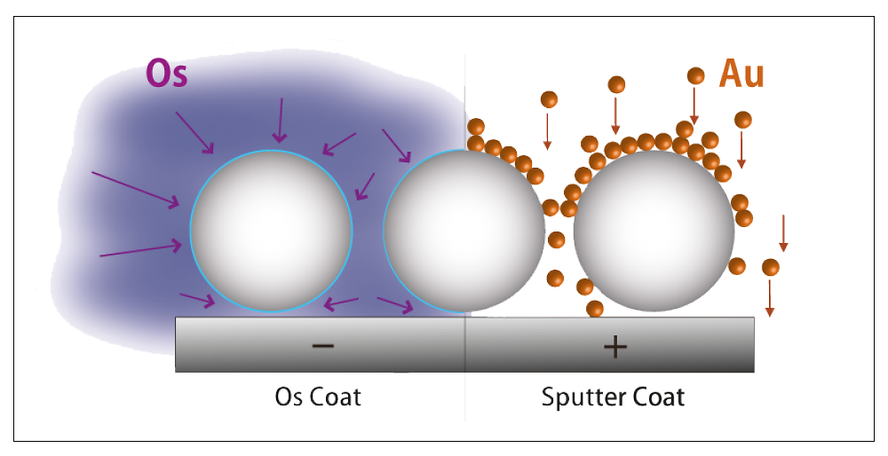
Isotropic Osmium Coating vs. anisotropic Sputter & Evaporation Coating
6. Variable Pressure Electron Staining (VPES) / Chemical Vapor Deposition (CVD) use reactive gases, such as osmium tetroxide (OsO₄) or ruthenium tetroxide (RuO₄), under controlled pressure conditions to form coatings that enhance image contrast, especially for high molecular weight polymers.
- Application: Ideal for contrast enhancement in EM, particularly with complex biological or polymer samples.
- Disadvantages: Requires specialized equipment and reactive chemicals
The appropriate coating method is critical for obtaining optimal imaging results in electron microscopy. The technique should be chosen based on sample composition, required resolution, and desired imaging outcomes.
We offer advanced sputter coating devices, such as the Luxor Au, Pt, and C coaters, as well as the Tennant 20, providing flexible solutions for various research and industrial requirements.
Sputter Coaters and Sputter Coating: An Overview
Sputter coating technology is foundational in both scientific research and industrial applications, particularly in materials science, microelectronics, and electron microscopy. This physical vapor deposition (PVD) technique deposits an ultra-thin film of material - typically metal - onto substrates to enhance surface conductivity, modify surface properties, or prepare samples for SEM.
At the core of this process is the sputter coater, a vacuum-based instrument. In operation, argon gas is introduced into a vacuum chamber and ionized. These positively charged argon ions are accelerated toward a negatively charged target material. Upon impact, atoms from the target are ejected and deposited onto the substrate, forming a coating layer.
Applications of Sputter Coating
- Scanning Electron Microscopy (SEM): Non-conductive samples are coated with conductive metals (e.g., gold, platinum)
- to prevent charging and improve image quality.
- Microelectronics: Creation of thin films and multilayer structures in semiconductor devices.
- Optics and Photonics: Deposition of functional and anti-reflective coatings.
- Decorative and Protective Coatings: Enhances aesthetic appeal in jewelry and adds durability to automotive parts.
Types of Sputter Targets
The choice of sputter target material defines the properties of the resulting thin film. With advancements in material science, a wide range of target materials are available:
Metallic Targets:
- Gold (Au): Excellent conductivity and chemical inertness; ideal for SEM preparation.
- Platinum (Pt): Produces fine-grain, stable coatings; used for high-resolution imaging.
- Chromium (Cr), Titanium (Ti), Aluminum (Al): Common in electronics and decorative applications.
Alloy Targets:
- Gold-Palladium (Au/Pd): Provides fine-grain conductive coatings for SEM.
- Nickel-Chromium (NiCr), Titanium Nitride (TiN): Used for specific electrical or mechanical properties.
Oxide Targets:
- Indium Tin Oxide (ITO): Transparent, conductive coatings used in display technologies.
- Zinc Oxide (ZnO): Utilized in gas sensors, photovoltaics, and transparent electronics.
Composite/Ceramic Targets:
- TiO₂, SiO₂, Al₂O₃: Used for optical, hard, or corrosion-resistant coatings. Suitable for applications requiring unique electrical, chemical, or optical properties.
In conclusion, sputter coating and related methods play a vital role in sample preparation for electron microscopy and in various industrial applications. The selection of the appropriate coating technique and target material is key to achieving optimal imaging performance and material functionality.