
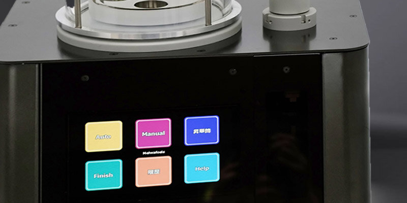
Tennant20 - Osmium-Beschichtungssystem
Nur ein hauchdünner Schleier trennt uns von neuen Entdeckungen.
Überwindet die Grenzen konventioneller REM-Bildgebung: Das in Japan entwickelte Tennant20 Osmium Coating System ermöglicht eine neue Dimension hochauflösender Elektronenmikroskopie.
Durch die Eliminierung der für Goldbeschichtungen typischen Körnungsartefakte entstehen artefakt- und aufladungsfreie REM-Aufnahmen. So wird die tatsächliche, unveränderte Morphologie selbst komplexer Nanostrukturen mit höchster Präzision sichtbar.
Sichtbarer Beweis
Osmium offenbart die wahre Oberflächenstruktur.
Beschl. Spannung 1,0kV Vergrößerung 30,000× Os Schichtdicke 5nm
Daten: SHIRAISHI CENTRAL LABORATORIES CO., LTD.
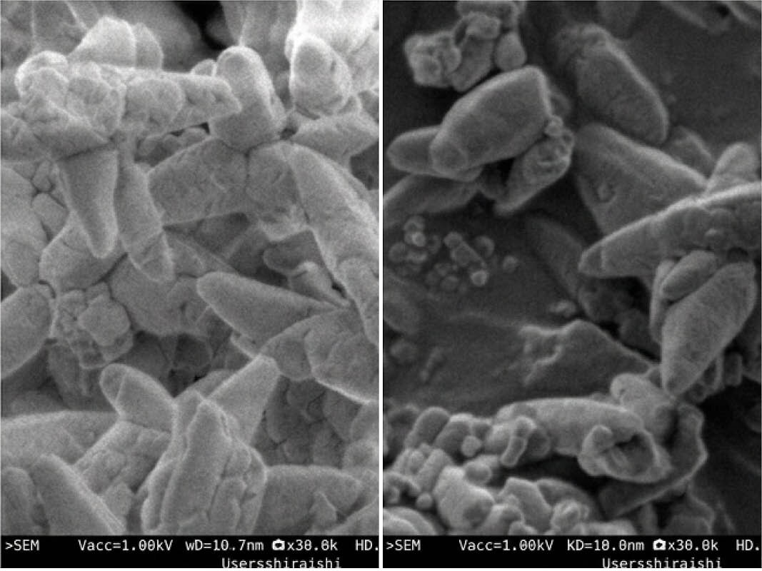
Platin Sputter Beschichtung
Osmium Beschichtung (Tennant20)
Methodik / Forschung
Durch Goldbeschichtung verborgene Nanostrukturen – jetzt sichtbar.
Was versteht man unter Osmium-Beschichtung?
Plasma CVD Osmium Beschichtung
Die Osmium-Beschichtung nutzt die plasmagestützte chemische Gasphasenabscheidung (Plasma-CVD), ein etabliertes Verfahren, um metallische Osmiumschichten mit einer Schichtdickenkontrolle im Nanometerbereich aufzubringen. Das Verfahren erzeugt hochhomogene, elektrisch leitfähige Beschichtungen bei niedrigen Prozesstemperaturen und gewährleistet gleichzeitig eine enorm hohe Reproduzierbarkeit der Schichtdicke.
Durch die Minimierung von Aufladungseffekten während der REM-Bildaufnahme und der Elementanalyse ermöglicht die Osmium-Beschichtung eine hochauflösende Darstellung feinster Oberflächenstrukturen mit hervorragender Bildqualität.
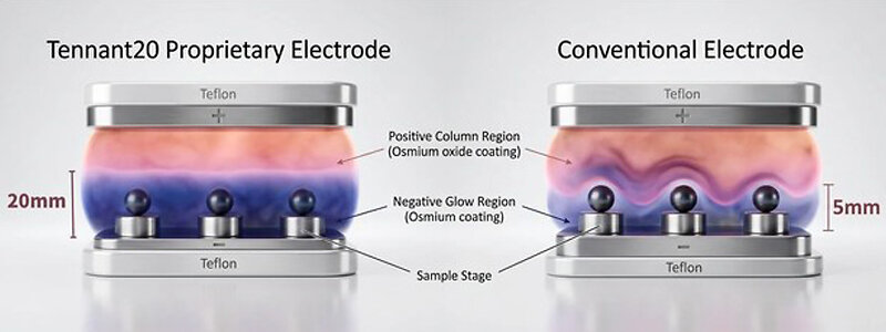
Bessere Beschichtungs-Qualität durch größeren Negativen Glimmphasenbereich
Die Abscheidung von metallischem Osmium erfolgt ausschließlich innerhalb des Negativen Glimmphasenbereichs des Plasmas. Bei konventionellen Parallelplatten-Elektrodensystemen erstreckt sich dieser Bereich nur bis etwa 5 mm über die Mitte des Probentisches, wodurch eine gleichmäßige Beschichtung von Proben mit komplexer Geometrie erheblich eingeschränkt wird.
Der Tennant20 verfügt über eine speziell entwickelte Elektrodenarchitektur, die den Negativen Glimmphasenbereich auf eine Höhe von 20 mm erweitert. Dieser deutlich vergrößerte Abscheidungsbereich ermöglicht eine stabile und homogene Osmiumbeschichtung – selbst bei Proben mit großen Höhenunterschieden.
Ab 0,5nm
Schichtdicke
Präzisionskontrolle im Nano-Bereich
20mm
Negativer Glimmphasenbereich
4x höher als konventionelle Systeme
20sec
Abscheidungszeit
Minimierung thermischer Defekte
1ms
Feedback Kontrolle
Maintains constant current
Vergleichende Daten – Klarheit schafft Fakten
Aufladung verdeckt das Wesentliche.
Aufladung
Bei herkömmlichen Sputter-Methoden, insbesondere beim Beschichten von komplexen, stark strukturierten Oberflächen kommt es häufig zu einer unvollständigen Beschichtung und dadurch zu einer Reduzierung der Proben-Leitfähigkeit. Dies führt während REM-Aufnahmen häufig zu lokalen Aufladungseffekten.
Im Gegensatz dazu, wird bei Osmium-Beschichtungen durch Gasphasenabscheidung eine homogene und kontinuierliche leitfähige Schicht erzeugt, die Aufladungsartefakte auf ein Minimum reduzieren und gerade bei komplexen Oberflächen-Geometrien eine stabile und hochauflösende Bildgebung ermöglicht.
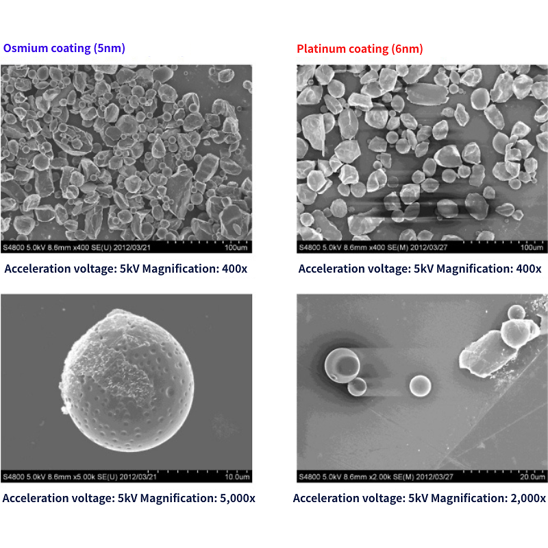
Unser Osmium-Beschichtungssystem gewährleistet eine hervorragende homogene Beschichtung – auch in sich überlappenden oder schwer zugänglichen Probenbereichen. Es verringert Aufladungseffekte zuverlässig und ermöglicht kontrastreiche Aufnahmen der gesamten Probe.
Dagegen weisen Gold-Sputterbeschichtungen in diesen Bereichen häufig eine unzureichende Schichtabdeckung auf. Die resultierenden Aufladungsartefakte führen häufig zu einer Reduktion der maximal erreichbaren Vergrößerung auf etwa 2.000x. Mit Osmium-Beschichtung sind dagegen stabile Aufnahmen bei Vergrößerungen von 5.000x und darüber hinaus erreichbar und somit die Visualisierung feinster Oberflächenstrukturen.
Data provided by Toyohashi University of Technology, Electronic Materials Course, Hiroyuki Muto
Gold maskiert die Oberfläche.
Körnungsartefakte
Bei Gold-Sputterbeschichtungen stammt ein Großteil der sichtbaren Oberflächenstruktur häufig von der Beschichtung selbst und nicht von der Probe selbst.
Osmium-Beschichtungen bilden eine extrem feinkörnige Metallschicht nahezu ohne körnungsbedingte Artefakte. Selbst bei Vergrößerungen bis zu 150.000-fach wird die tatsächliche Oberflächenmorphologie der Probe mit höchster Detailtreue dargestellt.
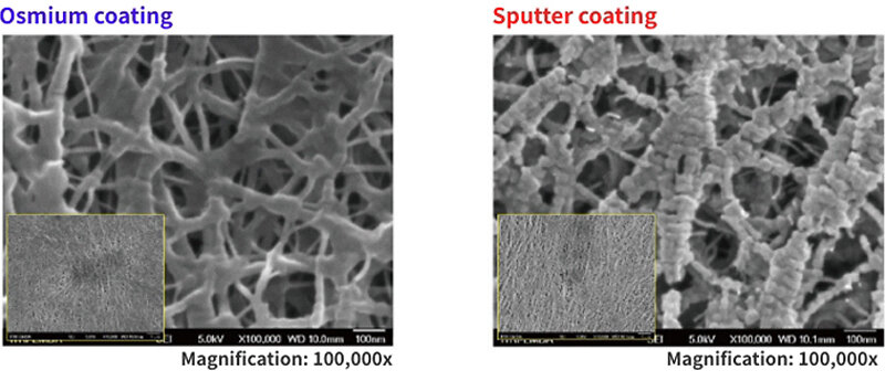
Polymerfilme
Bei Vergrößerung von 100.000x erzeugen Osmium-Beschichtung eine homogene und artefaktfreie Oberfläche, wodurch die ursprüngliche Morphologie der Probe erhalten bleibt. Platinbeschichtungen zeigen dagegen ausgeprägte Körnungen, welche feine Oberflächenstrukturen maskieren und die Bildqualität reduzieren.
Ultradünne Osmiumschichten mittels Plasma-CVD-Verfahren bei niedriger Prozesstemperatur ermöglichen hochauflösende REM-Aufnahmen ohne die für Platinbeschichtungen typischen Körnungsartefakte. Gleichzeitig wird durch die geringe thermische Belastung das Risiko einer wärmebedingten Schädigung temperaturempfindlicher organischer Materialien deutlich reduziert.
Data provided by Industrial Technology Research Institute (Taiwan)
Entwickelt zum Beschichten. Nicht zum Beschädigen.
Thermische Schädigungen
Konventionelle Sputterbeschichtungen können während des Beschichtungsprozesses eine thermische Belastung der Probe verursachen und dadurch empfindliche Strukturen verändern.
Mit einer Beschichtungszeit von nur 20 Sekunden minimieren Osmium-Beschichtungen den Wärmeeintrag und erhalten die ursprüngliche Morphologie der Probe, wodurch eine Aufnahme bei nahezu nativen Bedingungen ermöglicht werden.
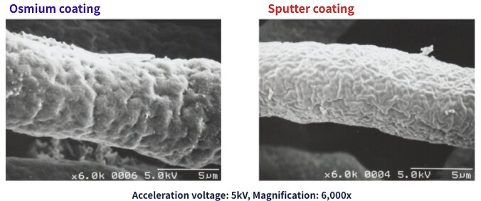
Vergleichende Aufnahmen eines Gefäßkorrosionspräparats eines Rattenherzens
Um Aufladungseffekte bei der Gold-Sputterbeschichtung ausreichend zu reduzieren, dauert der Sputter-Prozess etwa drei Minuten. Die lange Prozessdauer kann zu wärmebedingter Schrumpfung führen und erzeugt häufig relativ dicke und inhomogene Beschichtungen, welche feine Strukturen überdecken.
Osmium-Beschichtungen erzeugen hingegen ultradünne, homogene leitfähige Schichten innerhalb von nur 20 Sekunden. Somit werden Aufladungsartefakte vermieden und gleichzeitig bleibt die Proben-Morphologie für hochauflösende REM-Aufnahmen erhalten. Bereits bei 6.000-facher Vergrößerung wird die bessere Erhaltung feinster Oberflächenstrukturen deutlich sichtbar.
Data provided by Okayama University, Graduate School of Medicine, Dentistry and Pharmaceutical Sciences, Department of Human Morphology
Technologie
Design bestimmt das Ergebnis.
Der Tennant20 wurde entwickelt, um die konstruktionsbedingten Einschränkungen konventioneller Osmium-Beschichtungssysteme zu beseitigen.
Drei Schlüsseltechnologien sorgen für maximale Beschichtungsqualität, Reproduzierbarkeit und Sicherheit.

Patentierte Teflon-isolierte Elektrode
Eine speziell entwickelte, Teflon-isolierte Elektrode erweitert den Negativen Glimmphasenbereich, in dem die Osmiumabscheidung erfolgt, auf 20mm. Bei konventionellen Systemen beträgt dieser Bereich lediglich etwa 5mm.
Reproduzierbarkeit
Die Beschichtungsqualität sollte nicht von der Erfahrung des Anwenders abhängen.
Der Tennant20 verfügt über eine hochdynamische Regelung, welche Stromschwankungen im Millisekundenbereich kompensiert. Ergänzt durch eine 0,01 Sek. genaue Zeitsteuerung werden selbst ultradünne Schichten von 0,5nm präzise abgeschieden. Durch die Minimierung von Prozessschwankungen liefert das System stabile und reproduzierbare Beschichtungsergebnisse.
Sicherheit
Der Tennant20 wurde für eine sichere und kontrollierte Prozessgasführung entwickelt. Die vollständig geschlossene Prozesskammer sowie eine automatisierte Absaugsequenz entfernen nach der Beschichtung zuverlässig verbleibende Prozessgasrückstände. Anschließend wird die Kammer automatisch mit sauberer Luft geflutet.
Zusätzlich schließen speziell ausgelegte Sicherheits-Magnetventile bei einem Stromausfall selbstständig, wodurch ein unbeabsichtigter Gasaustritt verhindert, und ein sicherer Anlagenbetrieb gewährleistet wird.
Spezifikationen
Spezifikation & Qualität
Forschungsqualität in kompaktem Format.
Jedes Detail steht für die Qualität japanischer Ingenieurskunst.
Wichtige Merkmale
- Proprietäre PID-Regelung zur präzisen Stromregelung
- Automatisierte Absaugsequenz nach dem Beschichtungsprozess (Standard)
- Vollständig geschlossenes System mit Metallsublimationszylinder
- Protokollierung der Nutzungshistorie (bis zu 500 Datensätze)
- Passwortgeschützte Benutzerverwaltung
- Automatische Erinnerung zum Austausch der Osmium-Ampulle (werkzeugloser Wechsel)
- Austauschservice für Osmium-Ampullen (optional)
- Verschlusskappe für den Sublimationszylinder für sicheren Transport und Lagerung
Technische Daten
Weitere Informationen:

Tennant20
Produktseite, Broschüre & Datenblätter

Testbeschichtungen
Wir beschichten bis zu 3 Ihrer Proben für Sie kostenlos - desweiteren bieten wir auch Demos vor Ort an

Sicherheitskonzept
Erfahren Sie mehr über die Sicherheitshinweise

Kontakt
Für mehr Informationen können Sie gerne mit uns Kontakt aufnehmen.